Why Chips Below 7nm Depend on High-Purity Tantalum Targets
Leave a message
As semiconductor manufacturing moves below 7nm, materials are becoming just as important as transistor design itself. One of the biggest challenges in advanced chip production is controlling copper diffusion inside extremely small interconnect structures. Copper offers excellent electrical conductivity, which is why modern chips rely heavily on copper interconnect technology, but copper atoms are also highly mobile. Under thermal stress and long-term operation, they can gradually diffuse into surrounding dielectric and silicon layers, leading to leakage current, instability, and reduced chip reliability. At older process nodes this issue was easier to control, but below 7nm, where structures are measured in only a few nanometers, even minor atomic migration can directly affect yield and device performance.
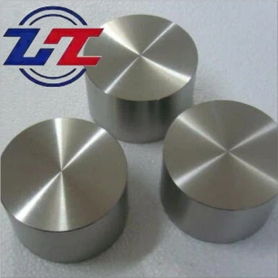
This is why high-purity tantalum barrier layers remain critical in advanced semiconductor manufacturing. Thin tantalum-based films are deposited between copper and surrounding structures to block diffusion while maintaining electrical stability. These layers are extremely thin, yet their performance directly influences interconnect reliability inside advanced chips. As the barrier layer itself becomes thinner, the purity requirements for tantalum targets become much stricter. Trace contamination, unstable grain structure, or inconsistent sputtering behavior can all affect film uniformity during PVD deposition. In advanced semiconductor production, even small fluctuations that were previously acceptable may now create wafer defects or reduce manufacturing yield. For this reason, semiconductor-grade tantalum targets require not only high purity, but also highly controlled density, grain size, and internal consistency throughout the entire manufacturing process.
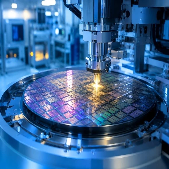


For tantalum material suppliers, the real difficulty is no longer simply producing tantalum metal. The challenge lies in maintaining stable processing quality from refining and electron beam melting to forging, machining, and final target fabrication. As AI chips, high-performance computing, and advanced packaging technologies continue increasing semiconductor complexity, demand for stable high-purity tantalum materials is expected to remain strong. In many ways, the growing importance of tantalum inside sub-7nm chips reflects a broader shift across the semiconductor industry: advanced manufacturing is increasingly limited not only by design capability, but also by materials engineering itself.
At Shaanxi Zhongheng Weichuang Metal, we focus on refractory and high-performance metal materials including tantalum, niobium, hafnium, tungsten, titanium, and related alloys for semiconductor, vacuum, aerospace, and high-temperature applications. If you are evaluating tantalum materials for sputtering targets or advanced industrial applications, our team can support both standard and custom processing requirements based on your technical specifications.Email: zhwctanbc103@163.com